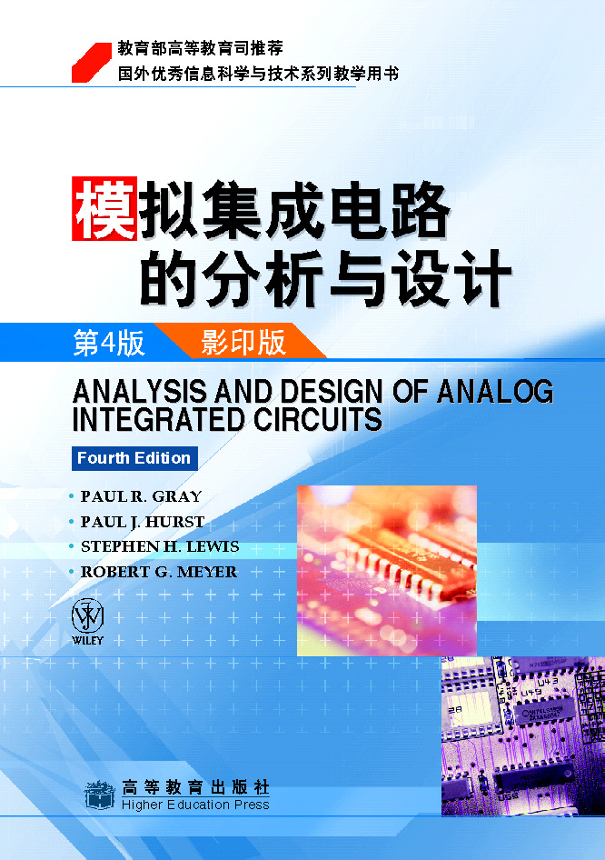
模拟集成电路的分析与设计 第4版
作者: Paul R. Gray 等
出版时间:2003-10-21
出版社:高等教育出版社
- 高等教育出版社
- 9787040130430
- 1
- 249661
- 平装
- 16开
- 2003-10-21
- 1000
- 896
CHAPTER 1
Models for Integrated-Circuit Active Devices
1.1 Introduction
1.2 Depletion Region of a pn Junction
1.2.1 Depletion-Region Capacitance
1.2.2 Junction Breakdown
1.3 Large-Signal Behavior of Bipolar Transistors
1.3.1 Large-Signal Models in the Forward-Active Region
1.3.2 Effects of Collector Voltage on Large-Signal Characteristics in the Forward-Active Region
1.3.3 Saturation and Inverse Active Regions
1.3.4 Transistor Breakdown Voltages
1.3.5 Dependence of Transistor Current Gain βF on Operating Conditions
1.4 Small-Signal Models of Bipolar Transistors
1.4.1 Transconductance
1.4.2 Base-Charging Capacitance
1.4.3 Input Resistance
1.4.4 Output Resistance
1.4.5 Basic Small-Signal Model of the Bipolar Transistor
1.4.6 Collector-Base Resistance
1.4.7 Parasitic Elements in the Small-Signal Model
1.4.8 Specification of Transistor Frequency Response
1.5 Large Signal Behavior of Metal-Oxide-Semiconductor Field-Effect Transistors
1.5.1 Transfer Characteristics of MOS Devices
1.5.2 Comparison of Operating Regions of Bipolar and MOS Transistors
1.5.3 Decomposition of Gate-Source Voltage
1.5.4 Threshold Temperature Dependence
1.5.5 MOS Device Voltage Limitations
1.6 Small-Signal Models of the MOS Transistors
1.6.1 Transconductance
1.6.2 Intrinsic Gate-Source and Gate-Drain Capacitance
1.6.3 Input Resistance
1.6.4 Output Resistance
1.6.5 Basic Small-Signal Model of the MOS Transistor
1.6.6 Body Transconductance
1.6.7 Parasitic Elements in the Small-Signal Model
1.6.8 MOS Transistor Frequency Response
1.7 Short-Channel Effects in MOS Transistors
1.7.1 Velocity Saturation from the Horizontal Field
1.7.2 Transconductance and Transition Frequency
1.7.3 Mobility Degradation from the Vertical Field
1.8 Weak Inversion in MOS Transistors
1.8.1 Drain Current in Weak Inversion
1.8.2 Transconductance and Transition Frequency in Weak Inversion
1.9 Substrate Current Flow in MOS Transistors
A.1.1 Summary of Active-Device Parameters
CHAPTER 2
Bipolar, MOS, and BiCMOS Integrated-Circuit Technology
2.1 Introduction
2.2 Basic Processes in Integrated-CircuitFabrication
2.2.1 Electrical Resistivity of Silicon
2.2.2 Solid-State Diffusion
2.2.3 Electrical Properties of DiffusedLayers
2.2.4 Photolithography
2.2.5 Epitaxial Growth
2.2.6 Ion Implantation
2.2.7 Local Oxidation
2.2.8 Polysilicon Deposition
2.3 High-Voltage Bipolar Integrated-Circuit Fabrication
2.4 Advanced Bipolar Integrated-Circuit Fabrication
2.5 Active Devices in Bipolar Analog Integrated Circuits
2.5.1 Integrated-Circuit npn Transistor
2.5.2 Integrated-Circuit pnp Transistors
2.6 Passive Components in Bipolar Integrated Circuits
2.6.1 Diffused Resistors
2.6.2 Epitaxial and Epitaxial Pinch Resistors
2.6.3 Integrated-Circuit Capacitors
2.6.4 Zener Diodes
2.6.5 Junction Diodes
2.7 Modifications to the Basic BipolarProcess
2.7.1 Dielectric Isolation
2.7.2 Compatible Processing for High-Performance Active Devices
2.7.3 High-Performance Passive Components
2.8 MOS Integrated-Circuit Fabrication
2.9 Active Devices in MOS Integrated Circuits
2.9.1 n-Channel Transistors
2.9.2 p-Channel Transistors
2.9.3 Depletion Devices
2.9.4 Bipolar Transistors
2.10 Passive Components in MOS Technology
2.10.1 Resistors
2.10.2 Capacitors in MOS Technology
2.10.3 Latchup in CMOS Technology
2.11 BiCMOS Technology
2.12 Heterojunction Bipolar Transistors
2.13 Interconnect Delay
2.14 Economics of Integrated-Circuit Fabrication
2.14.1 Yield Considerations in Integrated-Circuit Fabrication
2.14.2 Cost Considerations in Integrated-Circuit Fabrication
2.15 Packaging Considerations for Integrated Circuits
2.15.1 Maximum Power Dissipation
2.15.2 Reliability Considerations in Integrated-Circuit Packaging
A.2.1 SPICE Model-Parameter Files
CHAPTER 3
Single-Transistor and Multiple-TransistorAmplifiers
3.1 Device Model Selection for Approximate Analysis of Analog Circuits
3.2 Two-Port Modeling of Amplifiers
3.3 Basic Single-Transistor Amplifier Stages
3.3.1 Common-Emitter Configuration
3.3.2 Common-Source Configuration
3.3.3 Common-Base Configuration
3.3.4 Common-Gate Configuration
3.3.5 Common-Base and Common-Gate Configurations with Finite r。
3.3.5.1 Common-Base and Common-Gate Input Resistance
3.3.5.2 Common-Base and Common-Gate Output Resistance
3.3.6 Common-Collector Configuration (Emitter Follower)
3.3.7 Common-Drain Configuration (Source Follower)
3.3.8 Common-Emitter Amplifier with Emitter Degeneration
3.3.9 Common-Source Amplifier with Source Degeneration
3.4 Multiple-Transistor Amplifier Stages
3.4.1 The CC-CE, CC-CC, and Darlington Configurations
3.4.2 The Cascode Configuration
3.4.2.1 The Bipolar Cascode
3.4.2.2 The MOS Cascode
3.4.3 The Active Cascode
3.4.4 The Super Source Follower
3.5 Differential Pairs
3.5.1 The do Transfer Characteristic of an Emitter-Coupled Pair
3.5.2 The do Transfer Characteristic with Emitter Degeneration
3.5.3 The do Transfer Characteristic of a Source-Coupled Pair
3.5.4 Introduction to the Small-Signal Analysis of Differential Amplifiers
3.5.5 Small-Signal Characteristics of Balanced Differential Amplifiers
3.5.6 Device Mismatch Effects in Differential Amplifiers
3.5.6.1 Input Offset Voltage and Current
3.5.6.2 Input Offset Voltage of the Emitter-Coupled Pair
3.5.6.3 Offset Voltage of the Emitter-Coupled Pair: Approximate Analysis
3.5.6.4 Offset Voltage Drift in the Emitter-Coupled Pair
3.5.6.5 Input Offset Current of the Emitter-Coupled Pair
3.5.6.6 Input Offset Voltage of the Source-Coupled Pair
3.5.6.7 Offset Voltage of the Source-Coupled Pair: Approximate Analysis
3.5.6.8 Offset Voltage Drift in the Source-Coupled Pair
3.5.6.9 Small-Signal Characteristics of Unbalanced Differential Amplifiers
A.3.1 Elementary Statistics and the Gaussian Distribution
CHAPTER 4
Current Mirrors, Active Loads, and References
4.1 Introduction
4.2 Current Mirrors
4.2.1 General Properties
4.2.2 Simple Current Mirror
4.2.2.1 Bipolar
4.2.2.2 MOS
4.2.3 Simple Current Mirror with Beta Helper
4.2.3.1 Bipolar
4.2.3.2 MOS
4.2.4 Simple Current Mirror with Degeneration
4.2.4.1 Bipolar
4.2.4.2 MOS
4.2.5 Cascode Current Mirror
4.2.5.1 Bipolar
4.2.5.2 MOS
4.2.6 Wilson Current Mirror
4.2.6.1 Bipolar
4.2.6.2 MOS
4.3 Active Loads4.3.1 Motivation
4.3.2 Common-Emitter/Common-Source Amplifier with Complementary Load
4.3.3 Common-Emitter/Common-Source Amplifier with Depletion Load
4.3.4 Common-Emitter/Common-Source Amplifier with Diode-Connected Load
4.3.5 Differential Pair with Current-Mirror Load
4.3.5.1 Large-Signal Analysis
4.3.5.2 Small-Signal Analysis
4.3.5.3 Common-Mode Rejection Ratio
4.4 Voltage and Current References
4.4.1 Low-Current Biasing
4.4.1.1 Bipolar Widlar Current Source
4.4.1.2 MOS Widlar Current Source
4.4.1.3 Bipolar Peaking Current Source
4.4.1.4 MOS Peaking Current Source
4.4.2 Supply-Insensitive Biasing
4.4.2.1 Widlar Current Sources
4.4.2.2 Current Sources Using Other Voltage Standards
4.4.2.3 Self Biasing
4.4.3 Temperature-Insensitive Biasing
4.4.3.1 Band-Gap-Referenced Bias Circuits in Bipolar Technology
4.4.3.2 Band-Gap-Referenced Bias Circuits in CMOS Technology
A.4.1 Matching Considerations in Current Mirrors
A.4.1.1 Bipolar
A.4.1.2 MOS
A.4.2 Input Offset Voltage of Differential Pair with Active Load
A.4.2.1 Bipolar
A.4.2.2 MOS
CHAPTER 5
Output Stages
5.1 Introduction
5.2 The Emitter Follower As an Output Stage
5.2.1 Transfer Characteristics of the Emitter-Follower
5.2.2 Power Output and Efficiency
5.2.3 Emitter-Follower Drive Requirements
5.2.4 Small-Signal Properties of the Emitter Follower
5.3 The Source Follower As an Output Stage
5.3.1 Transfer Characteristics of the Source Follower
5.3.2 Distortion in the Source Follower
5.4 Class B Push-Pull Output Stage
5.4.1 Transfer Characteristic of the Class B Stage
5.4.2 Power Output and Efficiency of the Class B Stage
5.4.3 Practical Realizations of Class B Complementary Output Stages
5.4.4 All-npn Class B Output Stage
5.4.5 Quasi-Complementary Output Stages
5.4.6 Overload Protection
5.5 CMOS Class AB Output Stages
5.5.1 Common-Drain Configuration
5.5.2 Common-Source Configuration with Error Amplifiers
5.5.3 Alternative Configurations
5.5.3.1 Combined Common-Drain Common-Source Configuration
5.5.3.2 Combined Common-Drain Common-Source Configuration with High Swing
5.5.3.3 Parallel Common-Source Configuration
CHAPTER 6
Operational Amplifiers with Single-Ended Outputs
6.1 Applications of Operational Amplifiers
6.1.1 Basic Feedback Concepts
6.1.2 Inverting Amplifier
6.1.3 Noninverting Amplifier
6.1.4 Differential Amplifier
6.1.5 Nonlinear Analog Operations
6.1.6 Integrator, Differentiator
6.1.7 Internal Amplifiers
6.1.7.1 Switched-Capacitor Amplifier
6.1.7.2 Switched-Capacitor Integrator
6.2 Deviations from Ideality in Real Oper- ational Amplifiers
6.2.1 Input Bias Current
6.2.2 Input Offset Current
6.2.3 Input Offset Voltage
6.2.4 Common-Mode Input Range
6.2.5 Common-Mode Rejection Ratio (CMRR)
6.2.6 Power-Supply Rejection Ratio ( PSRR)
6.2.7 Input Resistance
6.2.8 Output Resistance
6.2.9 Frequency Response
6.2.10 Operational-Amplifier Equivalent Circuit
6.3 Basic Two-Stage MOS Operational Amplifiers
6.3.1 Input Resistance, Output Resistance, and Open-Circuit Voltage Gain
6.3.2 Output Swing
6.3.3 Input Offset Voltage
6.3.4 Common-Mode Rejection Ratio
6.3.5 Common-Mode Input Range
6.3.6 Power-Supply Rejection Ratio (PSRR)
6.3.7 Effect of Overdrive Voltages
6.3.8 Layout Considerations
6.4 Two-Stage MOS Operational Amplifiers with Cascodes
6.5 MOS Telescopic-Cascode Operational Amplifiers
6.6 MOS Folded-Cascode Operational Amplifiers
6.7 MOS Active-Cascode Operational Amplifiers
6.8 Bipolar Operational Amplifiers
6.8.1 The do Analysis of the 741 Operational Amplifier
6.8.2 Small-Signal Analysis of the 741 Operational Amplifier
6.8.3 Input Offset Voltage, Input Offset Current, and Common-Mode Rejection Ratio of the 741
6.9 Design Considerations for Bipolar Monolithic Operational Amplifiers
6.9.1 Design of Low-Drift Operational Amplifiers
6.9.2 Design of Low-Input-Current Operational Amplifiers
CHAPTER 7
Frequency Response of Integrated Circuits
7.1 Introduction
7.2 Single-Stage Amplifiers
7.2.1 Single-Stage Voltage Amplifiers and The Miller Effect
7.2.1.1 The Bipolar Differential Amplifier: DifferentialMode Gain
7.2.1.2 The MOS Differential Amplifier: DifferentialMode Gain
7.2.2 Frequency Response of the Common-Mode Gain for a Differential Amplifier
7.2.3 Frequency Response of Voltage Buffers
7.2.3.1 Frequency Response of the Emitter Follower
7.2.3.2 Frequency Response of the Source Follower
7.2.4 Frequency Response of Current Buffers
7.2.4.1 Common-Base-Amplifier Frequency Response
7.2.4.2 Common-Gate-Amplifier Frequency Response
7.3 Multistage Amplifier Frequency Response
7.3.1 Dominant-Pole Approximation
7.3.2 Zero-Value Time Constant Analysis
7.3.3 Cascode Voltage-Amplifier Frequency Response
7.3.4 Cascode Frequency Response
7.3.5 Frequency Response of a Current Mirror Loading a Differential Pair
7.3.6 Short-Circuit Time Constants
7.4 Analysis of the Frequency Response of the 741 Op Amp
7.4.1 High-Frequency Equivalent Circuit of the 741
7.4.2 Calculation of the -3-dB Frequency of the 741
7.4.3 Nondominant Poles of the 741
7.5 Relation Between Frequency Response and Time Response
CHAPTER 8
Feedback
8.1 Ideal Feedback Equation
8.2 Gain Sensitivity
8.3 Effect of Negative Feedback on Distortion
8.4 Feedback Configurations
8.4.1 Series-Shunt Feedback
8.4.2 Shunt-Shunt Feedback
8.4.3 Shunt-Series Feedback
8.4.4 Series-Series Feedback
8.5 Practical Configurations and the Effect of Loading
8.5.1 Shunt-Shunt Feedback
8.5.2 Series-Series Feedback
8.5.3 Series-Shunt Feedback
8.5.4 Shunt-Series Feedback
8.5.5 Summary
8.6 Single-Stage Feedback
8.6.1 Local Series Feedback
8.6.2 Local Shunt Feedback
8.7 The Voltage Regulator as a Feedback Circuit
8.8 Feedback Circuit Analysis Using Return Ratio
8.8.1 Closed-Loop Gain Using Return Ratio
8.8.2 Closed-Loop Impedance Formula Using Return Ratio
8.8.3 Summary-Return-Ratio Analysis
8.9 Modeling Input and Output Ports in Feedback Circuits
CHAPTER 9
Frequency Response and Stability of Feedback Amplifiers
9.1 Introduction
9.2 Relation Between Gain and Bandwidth in Feedback Amplifiers
9.3 Instability and the Nyquist Criterion
9.4 Compensation
9.4.1 Theory of Compensation
9.4.2 Methods of Compensation
9.4.3 Two-Stage MOS Amplifier Compensation
9.4.4 Compensation of Single-Stage CMOS OP Amps
9.4.5 Nested Miller Compensation
9.5 Root-Locus Techniques
9.5.1 Root Locus for a Three-Pole Transfer Function
9.5.2 Rules for Root-Locus Construction
9.5.3 Root Locus for Dominant-Pole Compensation
9.5.4 Root Locus for Feedback-Zero Compensation
9.6 Slew Rate
9.6.1 Origin of Slew-Rate Limitations
9.6.2 Methods of Improving Slew-Rate
9.6.3 Improving Slew-Rate in Bipolar Op Amps
9.6.4 Improving Slew-Rate in MOS Op Amps
9.6.5 Effect of Slew-Rate Limitations on Large-Signal Sinusoidal Performance
A.9.1 Analysis in Terms of Return-Ratio Parameters
A.9.2 Roots of a Quadratic Equation
CHAPTER 10
Nonlinear Analog Circuits
10.1 Introduction
10.2 Precision Rectification
10.3 Analog Multipliers Employing the Bipolar Transistor
10.3.1 The Emitter-Coupled Pair as a Simple Multiplier
10.3.2 The do Analysis of the Gilbert Multiplier Cell
10.3.3 The Gilbert Cell as an Analog Multiplier
10.3.4 A Complete Analog Multiplier
10.3.5 The Gilbert Multiplier Cell as a Balanced Modulator and Phase Dectector
10.4 Phase-Locked Loops (PLL)
10.4.1 Phase-Locked Loop Concepts
10.4.2 The Phase-Locked Loop in the Locked Condition
10.4.3 Integrated-Circuit Phase-Locked Loops
10.4.4 Analysis of the 560B Monolithic Phase-Locked Loop
10.5 Nonlinear Function Symbols
CHAPTER 11
Noise in Integrated Circuits
11.1 Introduction
11.2 Sources of Noise
11.2.1 Shot Noise
11.2.2 Thermal Noise
11.2.3 Flicker Noise(1/f Noise)
11.2.4 Burst Noise(Popcorn Noise)
11.2.5 Avalanche Noise
11.3 Noise Models of Integrated-Circuit Components
11.3.1 Junction Diode
11.3.2 Bipolar Transistor
11.3.3 MOS Transistor
11.3.4 Resistors
11.3.5 Capacitors and Inductors
11.4 Circuit Noise Calculations
11.4.1 Bipolar Transistor Noise Performance
11.4.2 Equivalent Input Noise and the Minimum Detectable Signal
11.5 Equivalent Input Noise Generators
11.5.1 Bipolar Transistor Noise Generators
11.5.2 MOS Transistor Noise Generators
11.6 Effect of Feedback on Noise Performance
11.6.1 Effect of Ideal Feedback on Noise Performance
11.6.2 Effect of Practical Feedback on Noise Performance
11.7 Noise Performance of Other Transistor Configurations
11.7.1 Common-Base Stage Noise Performance
11.7.2 Emitter-Follower Noise Performance
11.7.3 Differential-Pair Noise Performance
11.8 Noise in Operational Amplifiers
11.9 Noise Bandwidth
11.10 Noise Figure and Noise Temperature
11.10.1 Noise Figure
11.10.2 Noise Temperature
CHAPTER 12
Fully Differential Operational Amplifiers
12.1 Introduction
12.2 Properties of Fully Differential Amplifiers
12.3 Small-Signal Models for Balanced Differential Amplifiers
12.4 Common-Mode Feedback
12.4.1 Common-Mode Feedback at Low Frequencies
12.4.2 Stability and Compensation Considerations in a CMFB Loop
12.5 CMFB Circuits
12.5.1 CMFB Using Resistive Divider and Amplifier
12.5.2 CMFB Using Two Differential Pairs
12.5.3 CMFB Using Transistors in the Triode Region
12.5.4 Switched-Capacitor CMFB
12.6 Fully Differential Op Amps
12.6.1 A Fully Differential Two-Stage Op Amp
12.6.2 Fully Differential Telescopic Cascode Op Amp
12.6.3 Fully Differential Folded-Cascode Op Amp
12.6.4 A Differential Op Amp with Two Differential Input Stages
12.6.5 Neutralization
12.7 Unbalanced Fully Differential Circuits
12.8 Bandwidth of the CMFB Loop
Index

