

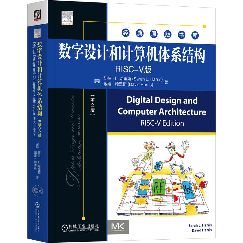


数字设计和计算机体系结构 RISC-V版(英文版) / 经典原版书库
定价:¥159.00
作者: [美]莎拉·L. 哈里斯(Sarah L. Harris) [美]戴维·哈里斯(David Harris)
出版时间:2025-03-10
出版社:机械工业出版社
- 机械工业出版社
- 9787111772569
- 1-1
- 2025-03-10
- 920
内容简介
继MIPS版和ARM版之后,本书与时俱进地推出了RISC-V版,将其作为核心处理器来介绍计算机体系结构的基本概念,涵盖数字逻辑设计的主要内容,并通过RISC-V处理器的设计强化数字逻辑的概念。书中采用一种独特的现代数字设计方法,先介绍数字逻辑门,接着讲述组合电路和时序电路的设计,并以这些基本的数字逻辑设计概念为基础,重点介绍如何设计实际的处理器。本书不仅反映了当前数字电路设计的主流方法,而且突出了计算机体系结构的工程特点。此外,大量示例及习题也可以加强读者对概念和技术的理解。本书适合高等院校计算机相关专业的学生阅读,也适合从事处理器设计的技术人员参考。
目录
Contents
Preface iv
About the Authors x
Chapter 1 From Zero to One 1
1.1 The Game Plan 1
1.2 The Art of Managing Complexity 2
1.2.1 Abstraction 2
1.2.2 Discipline 3
1.2.3 The Three -Y’s 4
1.3 The Digital Abstraction 5
1.4 Number Systems 7
1.4.1 Decimal Numbers 7
1.4.2 Binary Numbers 7
1.4.3 Hexadecimal Numbers 9
1.4.4 Bytes, Nibbles, and All That Jazz 11
1.4.5 Binary Addition 12
1.4.6 Signed Binary Numbers 13
1.5 Logic Gates 17
1.5.1 NOT Gate 18
1.5.2 Buffer 18
1.5.3 AND Gate 18
1.5.4 OR Gate 19
1.5.5 Other Two-Input Gates 19
1.5.6 Multiple-Input Gates 19
1.6 Beneath the Digital Abstraction 20
1.6.1 Supply Voltage 20
1.6.2 Logic Levels 20
1.6.3 Noise Margins 21
1.6.4 DC Transfer Characteristics 22
1.6.5 The Static Discipline 22
1.7 CMOS Transistors 24
1.7.1 Semiconductors 25
1.7.2 Diodes 25
1.7.3 Capacitors 26
1.7.4 nMOS and pMOS Transistors 26
1.7.5 CMOS NOT Gate 29
1.7.6 Other CMOS Logic Gates 29
1.7.7 Transmission Gates 31
1.7.8 Pseudo-nMOS Logic 31
1.8 Power Consumption 32
1.9 Summary and a Look Ahead 34
Exercises 36
Interview Questions 50
Chapter 2 Combinational Logic Design 53
2.1 Introduction 53
2.2 Boolean Equations 56
2.2.1 Terminology 56
2.2.2 Sum-of-Products Form 56
2.2.3 Product-of-Sums Form 58
2.3 Boolean Algebra 58
2.3.1 Axioms 59
2.3.2 Theorems of One Variable 59
2.3.3 Theorems of Several Variables 60
2.3.4 The Truth Behind It All 62
2.3.5 Simplifying Equations 63
2.4 From Logic to Gates 64
2.5 Multilevel Combinational Logic 67
2.5.1 Hardware Reduction 68
2.5.2 Bubble Pushing 69
2.6 X’s and Z’s, Oh My 71
2.6.1 Illegal Value: X 71
2.6.2 Floating Value: Z 72
2.7 Karnaugh Maps 73
2.7.1 Circular Thinking 74
2.7.2 Logic Minimization with K-Maps 75
2.7.3 Don’t Cares 79
2.7.4 The Big Picture 80
2.8 Combinational Building Blocks 81
2.8.1 Multiplexers 81
2.8.2 Decoders 84
2.9 Timing 86
2.9.1 Propagation and Contamination Delay 86
2.9.2 Glitches 90
2.10 Summary 93
Exercises 95
Interview Questions 104
Chapter 3 sequential Logic Design 107
3.1 Introduction 107
3.2 Latches and Flip-Flops 107
3.2.1 SR Latch 109
3.2.2 D Latch 111
3.2.3 D FIip-Flop 112
3.2.4 Register 112
3.2.5 Enabled Flip-Flop 113
3.2.6 Resettable Flip-Flop 114
3.2.7 Transistor-Level Latch and Flip-Flop
Designs 114
3.2.8 Putting It All Together 116
3.3 Synchronous Logic Design 117
3.3.1 Some Problematic Circuits 117
3.3.2 Synchronous Sequential Circuits 118
3.3.3 Synchronous and Asynchronous
Circuits 120
3.4 Finite State Machines 121
3.4.1 FSM Design Example 121
3.4.2 State Encodings 127
3.4.3 Moore and Mealy Machines 130
3.4.4 Factoring State Machines 132
3.4.5 Deriving an FSM from a Schematic 135
3.4.6 FSM Review 138
3.5 Timing of Sequential Logic 139
3.5.1 The Dynamic Discipline 140
3.5.2 System Timing 140
3.5.3 Clock Skew 146
3.5.4 Metastability 149
3.5.5 Synchronizers 150
3.5.6 Derivation of Resolution Time 152
3.6 Parallelism 155
3.7 Summary 159
Exercises 160
Interview Questions 169
Chapter 4 Hardware Description Languages 171
4.1 Introduction 171
4.1.1 Modules 171
4.1.2 Language Origins 172
4.1.3 Simulation and Synthesis 173
4.2 Combinational Logic 175
4.2.1 Bitwise Operators 175
4.2.2 Comments and White Space 178
4.2.3 Reduction Operators 178
4.2.4 Conditional Assignment 179
4.2.5 Internal Variables 180
4.2.6 Precedence 182
4.2.7 Numbers 183
4.2.8 Z’s and X’s 184
4.2.9 Bit Swizzling 186
4.2.10 Delays 186
4.3 Structural Modeling 188
4.4 Sequential Logic 191
4.4.1 Registers 191
4.4.2 Resettable Registers 192
4.4.3 Enabled Registers 194
4.4.4 Multiple Registers 195
4.4.5 Latches 196
4.5 More Combinational Logic 196
4.5.1 Case Statements 199
4.5.2 If Statements 200
4.5.3 Truth Tables with Don’t Cares 203
4.5.4 Blocking and Nonblocking Assignments 203
4.6 Finite State Machines 207
4.7 Data Types 211
4.7.1 SystemVerilog 212
4.7.2 VHDL 213
4.8 Parameterized Modules 215
4.9 Testbenches 218
4.10 Summary 222
Exercises 224
Interview Questions 235
Chapter 5 Digital Building Blocks 237
5.1 Introduction 237
5.2 Arithmetic Circuits 237
5.2.1 Addition 237
5.2.2 Subtraction 244
5.2.3 Comparators 245
5.2.4 ALU 247
5.2.5 Shifters and Rotators 251
5.2.6 Multiplication 253
5.2.7 Division 254
5.2.8 Further Reading 255
5.3 Number Systems 256
5.3.1 Fixed-Point Number Systems 256
5.3.2 Floating-Point Number Systems 257
5.4 Sequential Building Blocks 261
5.4.1 Counters 261
5.4.2 Shift Registers 262
5.5 Memory Arrays 265
5.5.1 Overview 265
5.5.2 Dynamic Random Access Memory (DRAM) 267
5.5.3 Static Random Access Memory (SRAM) 268
5.5.4 Area and Delay 268
5.5.5 Register Files 269
5.5.6 Read Only Memory (ROM) 269
5.5.7 Logic Using Memory Arrays 271
5.5.8 Memory HDL 272
5.6 Logic Arrays 272
5.6.1 Programmable Logic Array (PLA) 275
5.6.2 Field Programmable Gate Array (FPGA) 276
5.6.3 Array Implementations 282
5.7 Summary 283
Exercises 285
Interview Questions 297
Chapter 6 Architecture 299
6.1 Introduction 299
6.2 Assembly Language 300
6.2.1 Instructions 301
6.2.2 Operands: Registers, Memory, and Constants 302
6.3 Programming 308
6.3.1 Program Flow 308
6.3.2 Logical, Shift, and Multiply Instructions 308
6.3.3 Branching 311
6.3.4 Conditional Statements 313
6.3.5 Getting Loopy 315
6.3.6 Arrays 317
6.3.7 Function Calls 320
6.3.8 Pseudoinstructions 330
6.4 Machine Language 332
6.4.1 R-Type Instructions 332
6.4.2 I-Type Instructions 334
6.4.3 S/B-Type Instructions 336
6.4.4 U/J-Type Instructions 338
6.4.5 Immediate Encodings 340
6.4.6 Addressing Modes 341
6.4.7 Interpreting Machine Language Code 342
6.4.8 The Power of the Stored Program 343
6.5 Lights, Camera, Action: Compiling, Assembling,
and Loading 344
6.5.1 The Memory Map 344
6.5.2 Assembler Directives 346
6.5.3 Compiling 348
6.5.4 Assembling 350
6.5.5 Linking 353
6.5.6 Loading 355
6.6 Odds and Ends 355
6.6.1 Endianness 355
6.6.2 Exceptions 356
6.6.3 Signed and Unsigned Instructions 360
6.6.4 Floating-Point Instructions 361
6.6.5 Compressed Instructions 362
6.7 Evolution of the RISC-V Architecture 363
6.7.1 RISC-V Base Instruction Sets and Extensions 364
6.7.2 Comparison of RISC-Vand MIPS Architectures 365
6.7.3 Comparison of RISC-Vand ARM Architectures 365
6.8 Another Perspective: x86 Architecture 366
6.8.1 x86 Registers 366
6.8.2 x86 Operands 367
6.8.3 Status Flags 369
6.8.4 x86 Instructions 369
6.8.5 x86 Instruction Encoding 371
6.8.6 Other x86 Peculiarities 372
6.8.7 The Big Picture 373
6.9 Summary 374
Exercises 375
Interview Questions 390
Chapter 7 Microarchitecture 393
7.1 Introduction 393
7.1.1 Architectural State and Instruction Set 393
7.1.2 Design Process 394
7.1.3 Microarchitectures 396
7.2 Performance Analysis 397
7.3 Single-Cycle Processor 398
7.3.1 Sample Program 399
7.3.2 Single-Cycle Datapath 399
7.3.3 Single-Cycle Control 407
7.3.4 More Instructions 410
7.3.5 Performance Analysis 412
7.4 Multicycle Processor 415
7.4.1 Multicycle Datapath 416
7.4.2 Multicycle Control 422
7.4.3 More Instructions 432
7.4.4 Performance Analysis 435
7.5 Pipelined Processor 439
7.5.1 Pipelined Datapath 441
7.5.2 Pipelined Control 443
7.5.3 Hazards 443
7.5.4 Performance Analysis 454
7.6 HDL Representation 456
7.6.1 Single-Cycle Processor 457
7.6.2 Generic Building Blocks 461
7.6.3 Testbench 464
7.7 Advanced Microarchitecture 468
7.7.1 Deep Pipelines 468
7.7.2 Micro-Operations 469
7.7.3 Branch Prediction 470
7.7.4 Superscalar Processors 472
7.7.5 Out-of-Order Processor 473
7.7.6 Register Renaming 476
7.7.7 Multithreading 478
7.7.8 Multiprocessors 479
7.8 Real-World Perspective: Evolution of
RISC-V Microarchitecture 482
7.9 Summary 486
Exercises 488
Interview Questions 497
Chapter 8 Memory systems 499
8.1 Introduction 499
8.2 Memory System Performance Analysis 503
8.3 Caches 505
8.3.1 What Data is Held in the Cache? 505
8.3.2 How is Data Found? 506
8.3.3 What Data is Replaced? 514
8.3.4 Advanced Cache Design 515
8.4 Virtual Memory 519
8.4.1 Address Translation 522
8.4.2 The Page Table 523
8.4.3 The Translation Lookaside Buffer 525
8.4.4 Memory Protection 526
8.4.5 Replacement Policies 527
8.4.6 Multilevel Page Tables 527
8.5 Summary 530
Epilogue 530
Exercises 532
Interview Questions 541
Chapter 9 embedded I/O systems 542
9.1 Introduction 542
Appendix A Digital system Implementation 543
A.1 Introduction 543
Appendix B RIsC-V Instruction set summary 544
Appendix C C Programming 549
C.1 Introduction 549
Further Reading 551
Index 553
Preface iv
About the Authors x
Chapter 1 From Zero to One 1
1.1 The Game Plan 1
1.2 The Art of Managing Complexity 2
1.2.1 Abstraction 2
1.2.2 Discipline 3
1.2.3 The Three -Y’s 4
1.3 The Digital Abstraction 5
1.4 Number Systems 7
1.4.1 Decimal Numbers 7
1.4.2 Binary Numbers 7
1.4.3 Hexadecimal Numbers 9
1.4.4 Bytes, Nibbles, and All That Jazz 11
1.4.5 Binary Addition 12
1.4.6 Signed Binary Numbers 13
1.5 Logic Gates 17
1.5.1 NOT Gate 18
1.5.2 Buffer 18
1.5.3 AND Gate 18
1.5.4 OR Gate 19
1.5.5 Other Two-Input Gates 19
1.5.6 Multiple-Input Gates 19
1.6 Beneath the Digital Abstraction 20
1.6.1 Supply Voltage 20
1.6.2 Logic Levels 20
1.6.3 Noise Margins 21
1.6.4 DC Transfer Characteristics 22
1.6.5 The Static Discipline 22
1.7 CMOS Transistors 24
1.7.1 Semiconductors 25
1.7.2 Diodes 25
1.7.3 Capacitors 26
1.7.4 nMOS and pMOS Transistors 26
1.7.5 CMOS NOT Gate 29
1.7.6 Other CMOS Logic Gates 29
1.7.7 Transmission Gates 31
1.7.8 Pseudo-nMOS Logic 31
1.8 Power Consumption 32
1.9 Summary and a Look Ahead 34
Exercises 36
Interview Questions 50
Chapter 2 Combinational Logic Design 53
2.1 Introduction 53
2.2 Boolean Equations 56
2.2.1 Terminology 56
2.2.2 Sum-of-Products Form 56
2.2.3 Product-of-Sums Form 58
2.3 Boolean Algebra 58
2.3.1 Axioms 59
2.3.2 Theorems of One Variable 59
2.3.3 Theorems of Several Variables 60
2.3.4 The Truth Behind It All 62
2.3.5 Simplifying Equations 63
2.4 From Logic to Gates 64
2.5 Multilevel Combinational Logic 67
2.5.1 Hardware Reduction 68
2.5.2 Bubble Pushing 69
2.6 X’s and Z’s, Oh My 71
2.6.1 Illegal Value: X 71
2.6.2 Floating Value: Z 72
2.7 Karnaugh Maps 73
2.7.1 Circular Thinking 74
2.7.2 Logic Minimization with K-Maps 75
2.7.3 Don’t Cares 79
2.7.4 The Big Picture 80
2.8 Combinational Building Blocks 81
2.8.1 Multiplexers 81
2.8.2 Decoders 84
2.9 Timing 86
2.9.1 Propagation and Contamination Delay 86
2.9.2 Glitches 90
2.10 Summary 93
Exercises 95
Interview Questions 104
Chapter 3 sequential Logic Design 107
3.1 Introduction 107
3.2 Latches and Flip-Flops 107
3.2.1 SR Latch 109
3.2.2 D Latch 111
3.2.3 D FIip-Flop 112
3.2.4 Register 112
3.2.5 Enabled Flip-Flop 113
3.2.6 Resettable Flip-Flop 114
3.2.7 Transistor-Level Latch and Flip-Flop
Designs 114
3.2.8 Putting It All Together 116
3.3 Synchronous Logic Design 117
3.3.1 Some Problematic Circuits 117
3.3.2 Synchronous Sequential Circuits 118
3.3.3 Synchronous and Asynchronous
Circuits 120
3.4 Finite State Machines 121
3.4.1 FSM Design Example 121
3.4.2 State Encodings 127
3.4.3 Moore and Mealy Machines 130
3.4.4 Factoring State Machines 132
3.4.5 Deriving an FSM from a Schematic 135
3.4.6 FSM Review 138
3.5 Timing of Sequential Logic 139
3.5.1 The Dynamic Discipline 140
3.5.2 System Timing 140
3.5.3 Clock Skew 146
3.5.4 Metastability 149
3.5.5 Synchronizers 150
3.5.6 Derivation of Resolution Time 152
3.6 Parallelism 155
3.7 Summary 159
Exercises 160
Interview Questions 169
Chapter 4 Hardware Description Languages 171
4.1 Introduction 171
4.1.1 Modules 171
4.1.2 Language Origins 172
4.1.3 Simulation and Synthesis 173
4.2 Combinational Logic 175
4.2.1 Bitwise Operators 175
4.2.2 Comments and White Space 178
4.2.3 Reduction Operators 178
4.2.4 Conditional Assignment 179
4.2.5 Internal Variables 180
4.2.6 Precedence 182
4.2.7 Numbers 183
4.2.8 Z’s and X’s 184
4.2.9 Bit Swizzling 186
4.2.10 Delays 186
4.3 Structural Modeling 188
4.4 Sequential Logic 191
4.4.1 Registers 191
4.4.2 Resettable Registers 192
4.4.3 Enabled Registers 194
4.4.4 Multiple Registers 195
4.4.5 Latches 196
4.5 More Combinational Logic 196
4.5.1 Case Statements 199
4.5.2 If Statements 200
4.5.3 Truth Tables with Don’t Cares 203
4.5.4 Blocking and Nonblocking Assignments 203
4.6 Finite State Machines 207
4.7 Data Types 211
4.7.1 SystemVerilog 212
4.7.2 VHDL 213
4.8 Parameterized Modules 215
4.9 Testbenches 218
4.10 Summary 222
Exercises 224
Interview Questions 235
Chapter 5 Digital Building Blocks 237
5.1 Introduction 237
5.2 Arithmetic Circuits 237
5.2.1 Addition 237
5.2.2 Subtraction 244
5.2.3 Comparators 245
5.2.4 ALU 247
5.2.5 Shifters and Rotators 251
5.2.6 Multiplication 253
5.2.7 Division 254
5.2.8 Further Reading 255
5.3 Number Systems 256
5.3.1 Fixed-Point Number Systems 256
5.3.2 Floating-Point Number Systems 257
5.4 Sequential Building Blocks 261
5.4.1 Counters 261
5.4.2 Shift Registers 262
5.5 Memory Arrays 265
5.5.1 Overview 265
5.5.2 Dynamic Random Access Memory (DRAM) 267
5.5.3 Static Random Access Memory (SRAM) 268
5.5.4 Area and Delay 268
5.5.5 Register Files 269
5.5.6 Read Only Memory (ROM) 269
5.5.7 Logic Using Memory Arrays 271
5.5.8 Memory HDL 272
5.6 Logic Arrays 272
5.6.1 Programmable Logic Array (PLA) 275
5.6.2 Field Programmable Gate Array (FPGA) 276
5.6.3 Array Implementations 282
5.7 Summary 283
Exercises 285
Interview Questions 297
Chapter 6 Architecture 299
6.1 Introduction 299
6.2 Assembly Language 300
6.2.1 Instructions 301
6.2.2 Operands: Registers, Memory, and Constants 302
6.3 Programming 308
6.3.1 Program Flow 308
6.3.2 Logical, Shift, and Multiply Instructions 308
6.3.3 Branching 311
6.3.4 Conditional Statements 313
6.3.5 Getting Loopy 315
6.3.6 Arrays 317
6.3.7 Function Calls 320
6.3.8 Pseudoinstructions 330
6.4 Machine Language 332
6.4.1 R-Type Instructions 332
6.4.2 I-Type Instructions 334
6.4.3 S/B-Type Instructions 336
6.4.4 U/J-Type Instructions 338
6.4.5 Immediate Encodings 340
6.4.6 Addressing Modes 341
6.4.7 Interpreting Machine Language Code 342
6.4.8 The Power of the Stored Program 343
6.5 Lights, Camera, Action: Compiling, Assembling,
and Loading 344
6.5.1 The Memory Map 344
6.5.2 Assembler Directives 346
6.5.3 Compiling 348
6.5.4 Assembling 350
6.5.5 Linking 353
6.5.6 Loading 355
6.6 Odds and Ends 355
6.6.1 Endianness 355
6.6.2 Exceptions 356
6.6.3 Signed and Unsigned Instructions 360
6.6.4 Floating-Point Instructions 361
6.6.5 Compressed Instructions 362
6.7 Evolution of the RISC-V Architecture 363
6.7.1 RISC-V Base Instruction Sets and Extensions 364
6.7.2 Comparison of RISC-Vand MIPS Architectures 365
6.7.3 Comparison of RISC-Vand ARM Architectures 365
6.8 Another Perspective: x86 Architecture 366
6.8.1 x86 Registers 366
6.8.2 x86 Operands 367
6.8.3 Status Flags 369
6.8.4 x86 Instructions 369
6.8.5 x86 Instruction Encoding 371
6.8.6 Other x86 Peculiarities 372
6.8.7 The Big Picture 373
6.9 Summary 374
Exercises 375
Interview Questions 390
Chapter 7 Microarchitecture 393
7.1 Introduction 393
7.1.1 Architectural State and Instruction Set 393
7.1.2 Design Process 394
7.1.3 Microarchitectures 396
7.2 Performance Analysis 397
7.3 Single-Cycle Processor 398
7.3.1 Sample Program 399
7.3.2 Single-Cycle Datapath 399
7.3.3 Single-Cycle Control 407
7.3.4 More Instructions 410
7.3.5 Performance Analysis 412
7.4 Multicycle Processor 415
7.4.1 Multicycle Datapath 416
7.4.2 Multicycle Control 422
7.4.3 More Instructions 432
7.4.4 Performance Analysis 435
7.5 Pipelined Processor 439
7.5.1 Pipelined Datapath 441
7.5.2 Pipelined Control 443
7.5.3 Hazards 443
7.5.4 Performance Analysis 454
7.6 HDL Representation 456
7.6.1 Single-Cycle Processor 457
7.6.2 Generic Building Blocks 461
7.6.3 Testbench 464
7.7 Advanced Microarchitecture 468
7.7.1 Deep Pipelines 468
7.7.2 Micro-Operations 469
7.7.3 Branch Prediction 470
7.7.4 Superscalar Processors 472
7.7.5 Out-of-Order Processor 473
7.7.6 Register Renaming 476
7.7.7 Multithreading 478
7.7.8 Multiprocessors 479
7.8 Real-World Perspective: Evolution of
RISC-V Microarchitecture 482
7.9 Summary 486
Exercises 488
Interview Questions 497
Chapter 8 Memory systems 499
8.1 Introduction 499
8.2 Memory System Performance Analysis 503
8.3 Caches 505
8.3.1 What Data is Held in the Cache? 505
8.3.2 How is Data Found? 506
8.3.3 What Data is Replaced? 514
8.3.4 Advanced Cache Design 515
8.4 Virtual Memory 519
8.4.1 Address Translation 522
8.4.2 The Page Table 523
8.4.3 The Translation Lookaside Buffer 525
8.4.4 Memory Protection 526
8.4.5 Replacement Policies 527
8.4.6 Multilevel Page Tables 527
8.5 Summary 530
Epilogue 530
Exercises 532
Interview Questions 541
Chapter 9 embedded I/O systems 542
9.1 Introduction 542
Appendix A Digital system Implementation 543
A.1 Introduction 543
Appendix B RIsC-V Instruction set summary 544
Appendix C C Programming 549
C.1 Introduction 549
Further Reading 551
Index 553
