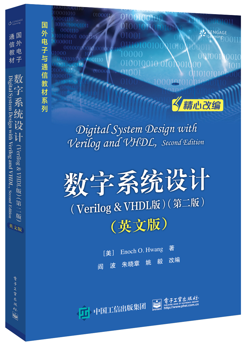
- 电子工业出版社
- 9787121334214
- 1-1
- 295108
- 16开
- 2018-01
- 420
- 电子信息工程(工学/理学)
- 本科 研究生(硕士、EMBA、MBA、MPA、博士)
Chapter 1 Introduction to Microprocessor Design
1.1 Overview of Microprocessor Design
1.2 Design Abstraction Levels
1.3 Examples of a 2-to-1 Multiplexer
1.3.1 Behavioral Level
1.3.2 Gate Level
1.3.3 Transistor Level
1.4 Introduction to Hardware Description Language
1.5 Synthesis
1.6 Going Forward
1.7 Problems
Chapter 2 Fundamentals of Digital Circuits
2.1 Binary Numbers
2.1.1 Counting in Binary
2.1.2 Converting between Binary and Decimal
2.1.3 Octal and Hexadecimal Notations
2.1.4 Binary Number Arithmetic
2.2 Negative Numbers
2.2.1 Two’s Complement Representation
2.2.2 Sign Extension
2.2.3 Signed Number Arithmetic
2.3 Binary Switch
2.4 Basic Logic Operators and Logic Expressions
2.5 Logic Gates
2.6 Truth Tables
2.7 Boolean Algebra and Boolean Equations
2.7.1 Boolean Algebra
2.7.2 Duality Principle
2.7.3 Boolean Functions and Their Inverses
2.8 Minterms and Maxterms
2.8.1 Minterms
2.8.2 Maxterms
2.9 Canonical, Standard, and Non-Standard Forms
2.10 Digital Circuits
2.11 Designing a Car Security System
2.12 Verilog and VHDL Code for Digital Circuits
2.12.1 Verilog Code for a Boolean Function
2.12.2 VHDL Code for a Boolean Function
2.13 Problems
Chapter 3 Combinational Circuits 65
3.1 Analysis of Combinational Circuits
3.1.1 Using a Truth Table
3.1.2 Using a Boolean Function
3.2 Synthesis of Combinational Circuits
3.2.1 Using Only NAND Gates
3.3 Minimization of Combinational Circuits
3.3.1 Boolean Algebra
3.3.2 Karnaugh Maps
3.3.3 Don’t-Cares
3.3.4 Tabulation Method
3.4 Timing Hazards and Glitches
3.4.1 Using Glitches
3.5 BCD to 7-Segment Decoder
3.6 Verilog and VHDL Code for Combinational Circuits
3.6.1 Structural Verilog Code
3.6.2 Structural VHDL Code
3.6.3 Dataflow Verilog Code
3.6.4 Dataflow VHDL Code
3.6.5 Behavioral Verilog Code
3.6.6 Behavioral VHDL Code
3.7 Problems
Chapter 4 Standard Combinational Components
4.1 Signal Naming Conventions
4.2 Multiplexer
4.3 Adder
4.3.1 Full Adder
4.3.2 Ripple-Carry Adder
4.3.3 Carry-Lookahead Adder
4.4 Subtractor
4.5 Adder-Subtractor Combination
4.6 Arithmetic Logic Unit
4.7 Decoder
4.8 Tri-State Buffer
4.9 Comparator
4.10 Shifter
4.11 Multiplier
4.12 Problems
Chapter 5 Sequential Circuits
5.1 Bistable Element
5.2 SR Latch
5.3 Car Security System―Version 2
5.4 SR Latch with Enable
5.5 D Latch
5.6 D Latch with Enable
5.7 Verilog and VHDL Code for Memory Elements
5.7.1 VHDL Code for a D Latch with Enable
5.7.2 Verilog Code for a D Latch with Enable
5.8 Clock
5.9 D Flip-Flop
5.9.1 Alternative Smaller Circuit
5.10 D Flip-Flop with Enable
5.10.1 Asynchronous Inputs
5.11 Description of a Flip-Flop
5.11.1 Characteristic Table
5.11.2 Characteristic Equation
5.11.3 State Diagram
5.12 Register
5.13 Register File
5.14 Memories
5.14.1 ROM
5.14.2 RAM
5.15 Shift Registers
5.15.1 Serial-to-Parallel Shift Register
5.15.2 Serial-to-Parallel and Parallel-to-Serial Shift Register
5.15.3 Linear Feedback Shift Register
5.16 Counters
5.16.1 Binary Up Counter
5.16.2 Binary Up Counter with Parallel Load
5.17 Timing Issues
5.18 Problems
Chapter 6 Finite-State Machines
6.1 Finite-State Machine Models
6.2 State Diagrams
6.3 Analysis of Finite-State Machines
6.3.1 Next-State Equations
6.3.2 Next-State Table
6.3.3 Output Equations
6.3.4 Output Table
6.3.5 State Diagram
6.3.6 Example
6.4 Synthesis of Finite-State Machines
6.4.1 State Diagram
6.4.2 Next-State Table
6.4.3 Next-State Equations
6.4.4 Output Table and Output Equations
6.4.5 FSM Circuit
6.5 Optimizations for FSMs
6.5.1 State Reduction
6.5.2 State Encoding
6.5.3 Unused States
6.6 FSM Construction Examples
6.6.1 Car Security System―Version 3
6.6.2 Modulo-6 Up-Counter
6.6.3 One-Shot Circuit
6.6.4 Simple Microprocessor Control Unit
6.6.5 Elevator Controller Using a Moore FSM
6.6.6 Elevator Controller Using a Mealy FSM
6.7 Verilog and VHDL Code for FSM Circuits
6.7.1 Behavioral Verilog Code for a Moore FSM
6.7.2 Behavioral Verilog Code for a Mealy FSM
6.7.3 Behavioral VHDL Code for a Moore FSM
6.7.4 Behavioral VHDL Code for a Mealy FSM
6.8 Problems
Chapter 7 Dedicated Microprocessors
7.1 Need for a Datapath
7.2 Constructing the Datapath
7.2.1 Selecting Registers
7.2.2 Selecting Functional Units
7.2.3 Data Transfer Methods
7.2.4 Generating Status Signals
7.3 Constructing the Control Unit
7.3.1 Deriving the Control Signals
7.3.2 Deriving the State Diagram
7.3.3 Timing Issues
7.3.4 Deriving the FSM Circuit
7.4 Constructing the Complete Microprocessor
7.5 Dedicated Microprocessor Construction Examples
7.5.1 Greatest Common Divisor
7.5.2 High-Low Number Guessing Game
7.5.3 Traffic Light Controller
7.6 Verilog and VHDL Code for Dedicated Microprocessors
7.6.1 FSM1D Model
7.6.2 FSMD Model
7.6.3 Algorithmic Model
7.7 Problems
Chapter 8 General-Purpose Microprocessors
8.1 Overview of the CPU Design
8.2 The EC-1 General-Purpose Microprocessor
8.2.1 Instruction Set
8.2.2 Datapath
8.2.3 Control Unit
8.2.4 Complete Circuit
8.2.5 Sample Program
8.2.6 Simulation
8.2.7 Hardware Implementation
8.3 The EC-2 General-Purpose Microprocessor
8.3.1 Instruction Set
8.3.2 Datapath
8.3.3 Control Unit
8.3.4 Complete Circuit
8.3.5 Sample Program
8.3.6 Hardware Implementation
8.4 Extending the EC-2 Instruction Set
Chapter 9 Interfacing Microprocessors
9.1 Multiplexing 7-Segment LED Display
9.1.1 Theory of Operation
9.1.2 Controller Design
9.2 Issues with Interfacing Switches
9.3 3×4 Keypad Controller
9.3.1 Theory of Operation
9.3.2 Controller Design


